Lab 1 - Signal Synthesis and Simulation
Note
Estimated Time to Complete: 2.5-3 hours
Using Xilinx Vivado’s Simulation functionality is critical to design and debugging of signal processing blocks. We use Direct Digital Synthesis (DDS) as an example to generate a tone (sine wave) as a baseline example in this lab. Imagine you’re a painter, but instead of a brush and paint, you’re equipped with numbers and math. Your canvas? The world of digital signals. In this vibrant world, Direct Digital Synthesis (DDS) is your superpower. With DDS, you can conjure up any waveform you desire—sine waves, square waves, and everything in between—just by crunching some numbers.
Picture it as a magical music box: you turn the crank (input a frequency), and out comes a beautiful, pristine wave, ready to serenade the digital world. And the best part? You’re the maestro, conducting your waves with pinpoint accuracy, adjusting the tempo (frequency) and volume (amplitude) at your will, all in real-time.
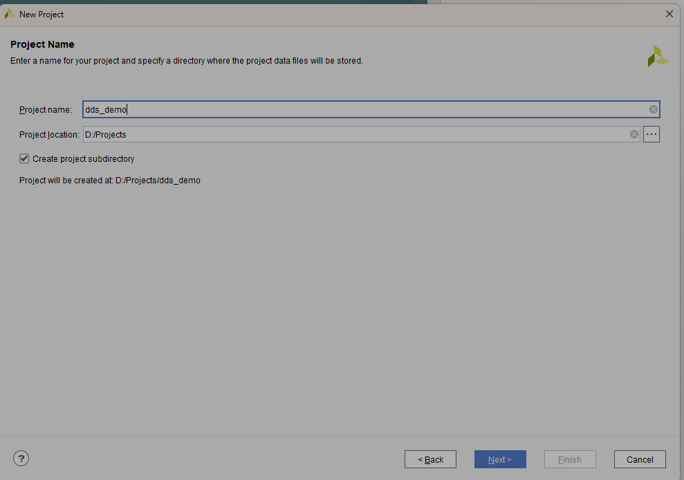
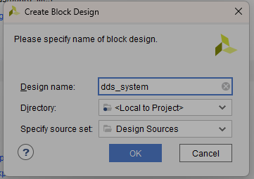
Open Vivado and press Create Project,
click Next and name the project.
Keep defaults on next screen RTL Project, Click Next.
No sources to add, Click Next.
No constraints to add Click Next
Click Boards, and scroll down to find the ZCU 111 Evaluation Board, Click Next.
Click Finish
The DDS Compiler Block
Note
Understanding of this block is critical to signal synthesis and design, take your time to understand, documentation from AMD/Xilinx is worth the read.
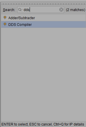
Vivado should now open your new project. Click Create Block Design in the left column, Click *OK*.
The block design window opens, Click on the + icon to add an IP core.
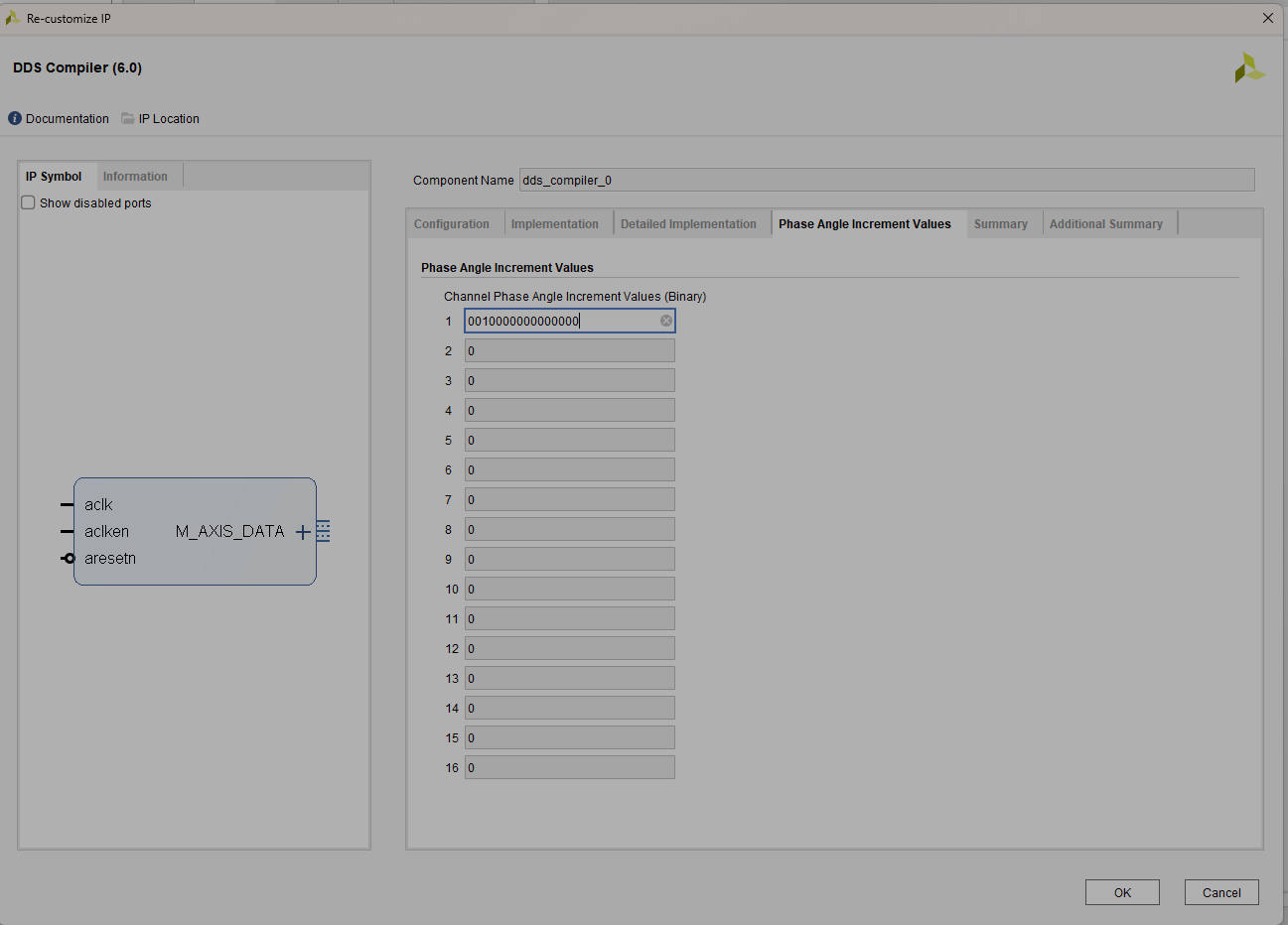
Double click the DDS block that you just added. Set parameters accordingly. The binary number should be 16 bits long, the third bit is 1. `0010000000000000`.
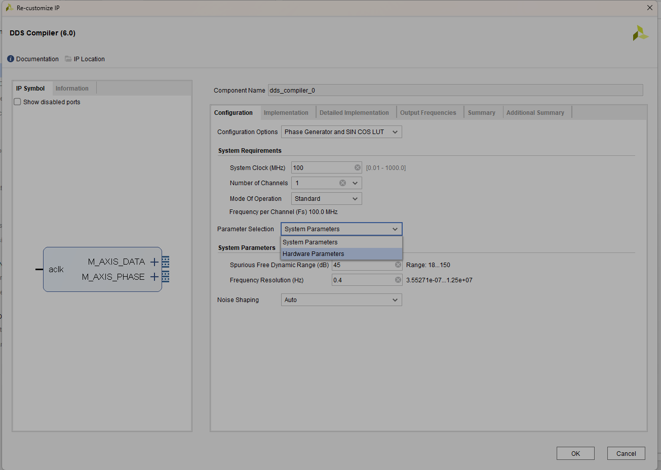
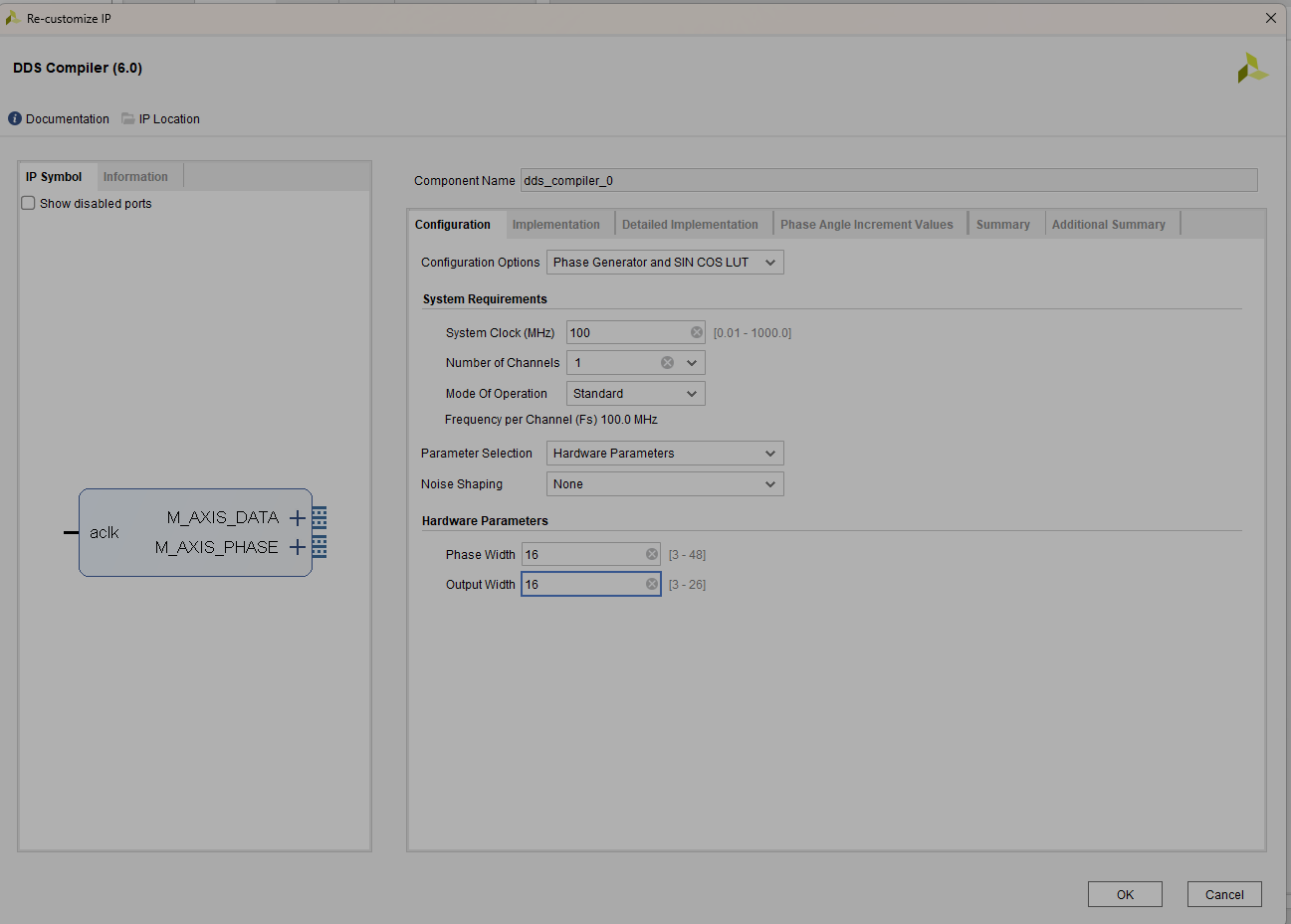
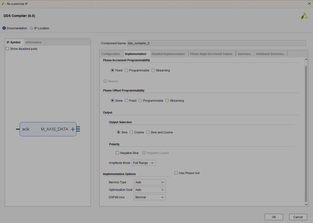
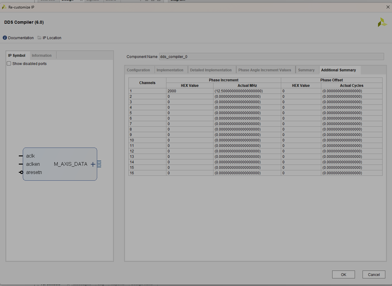
Click OK
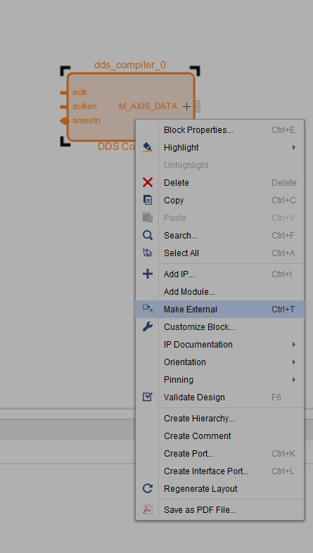
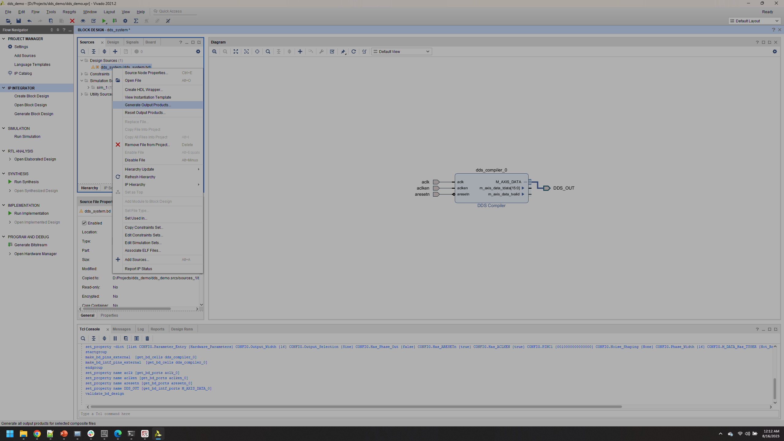
Right click your DDS block and click Make External, this allows your block to connect to outside sources by automatically adding ports.
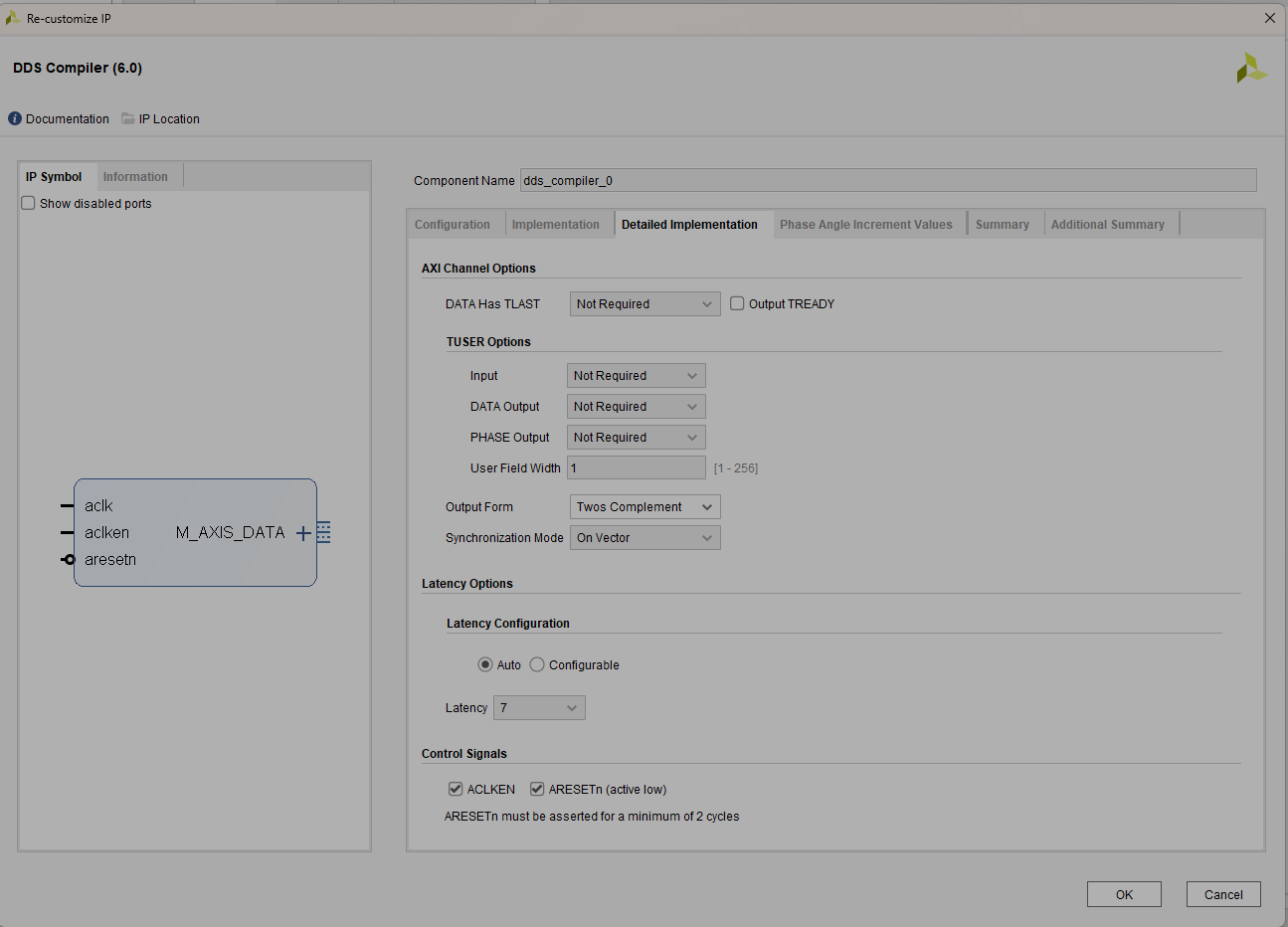
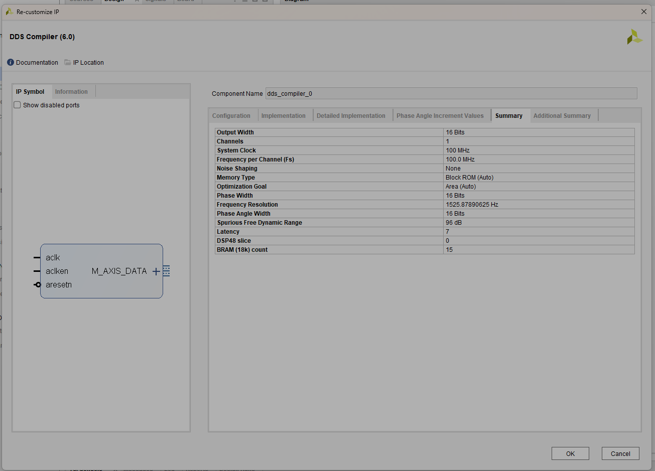
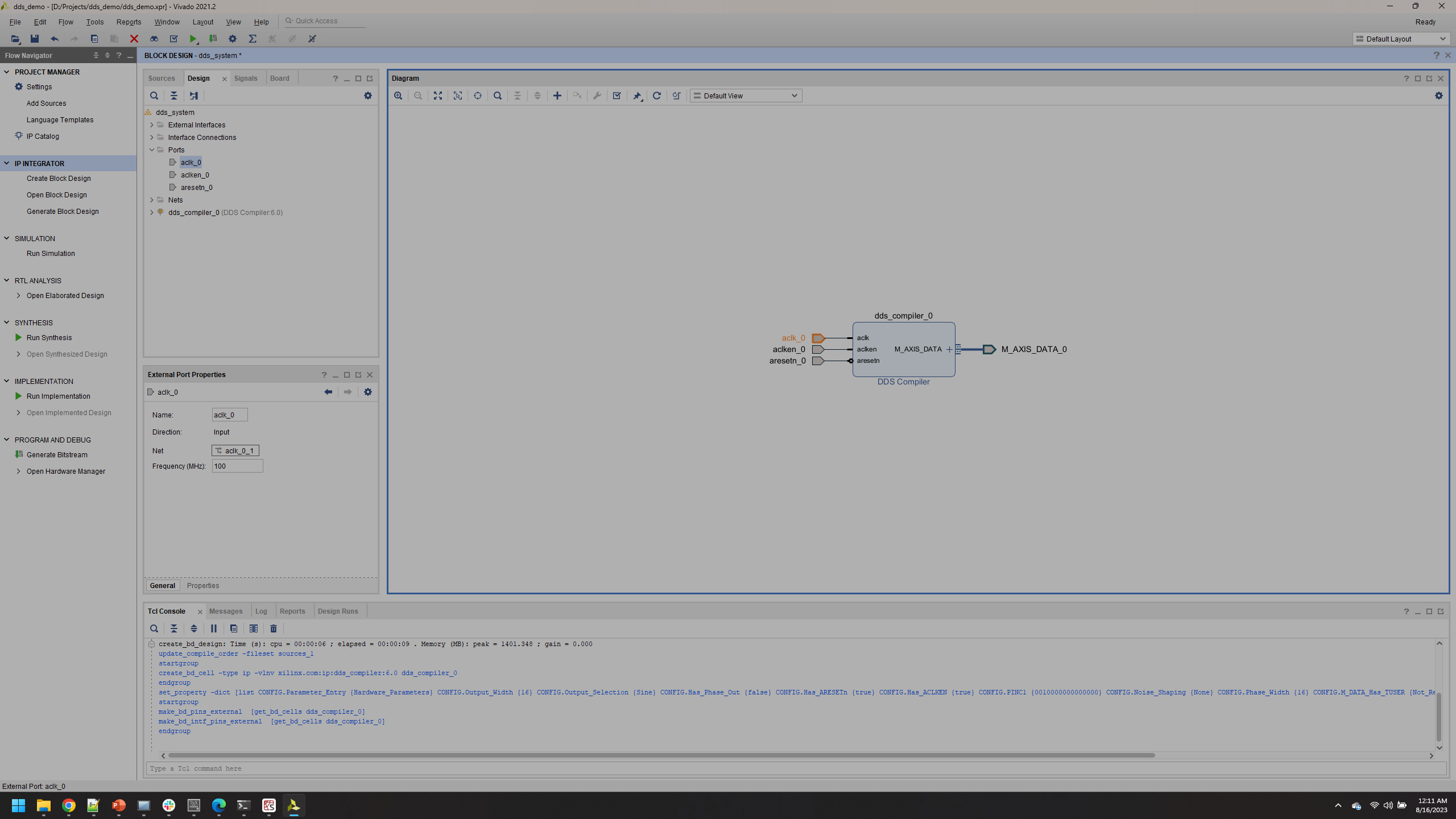
You an view the properties of each port by click on them. Note the frequency of this clock is 100 MHz. You also use this to change the name of ports
Note
Important: Port names are critical for properly interfacing, name it something that makes sense for your design.
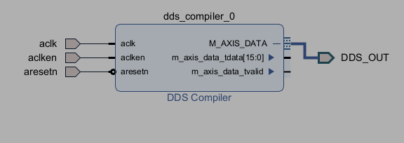
A suggested naming scheme is shown below, suggested because the later code you use has these as the main port names. You can press the + to expand the M_AXIS_DATA port.
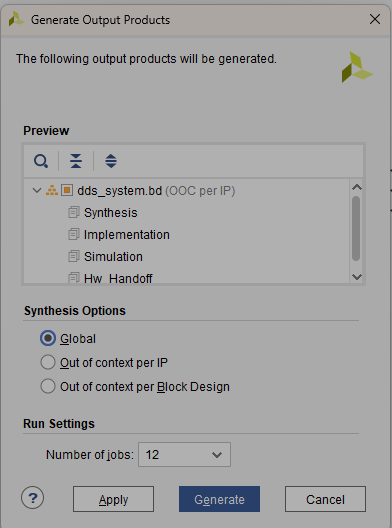
Once the port names are changed, go ahead and right click the block design in the Design Sources list and click Generate Output Products
Change to Global if it is not, and click Generate.
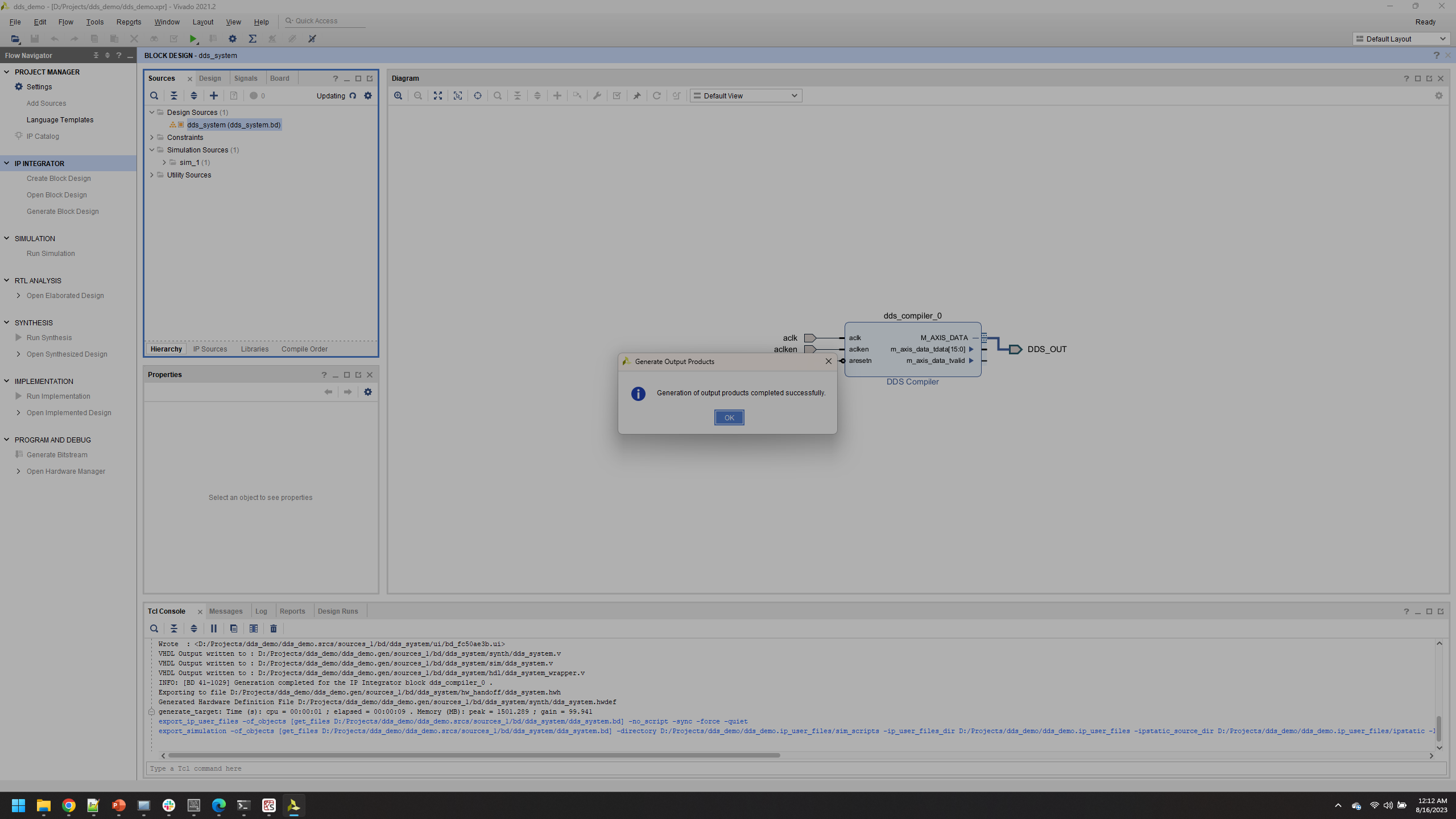
Click OK once prompted after output products are generated.
right click the block design in the Design Sources list and click Create HDL Wrapper
Running a Simulation
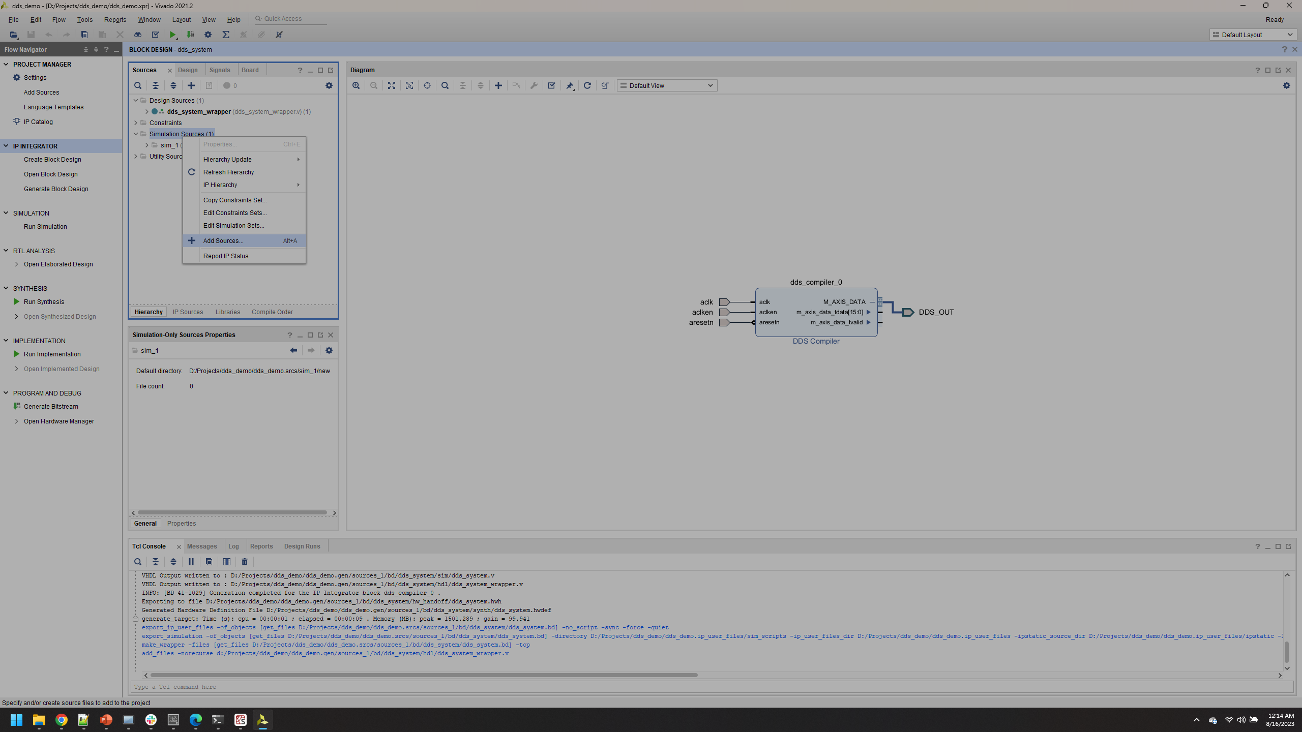
Right click Simulation Resources and click Add Sources, click Create File.
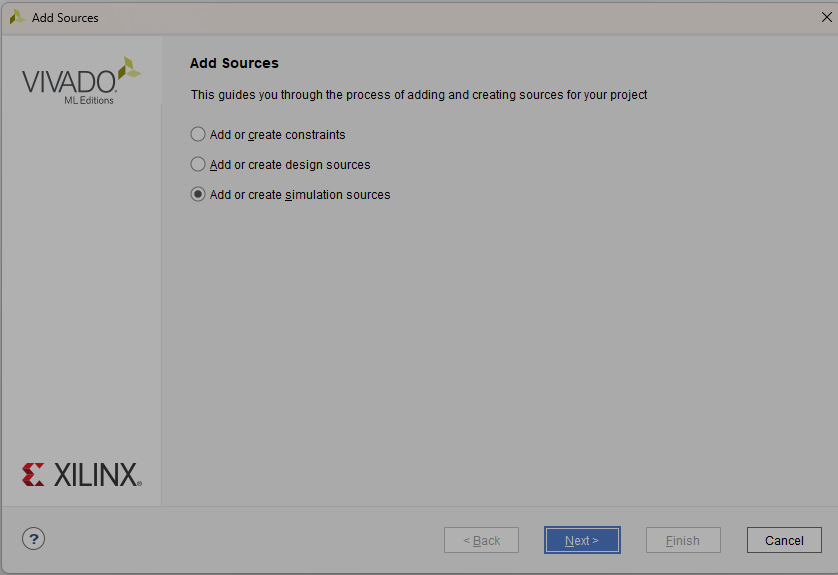
Click Next
Name the file tb (for testbench).
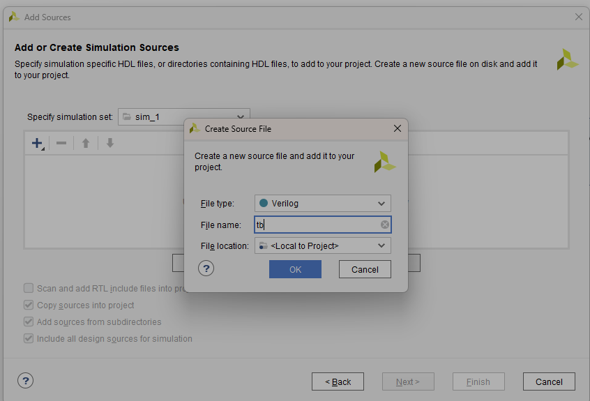
Click Ok
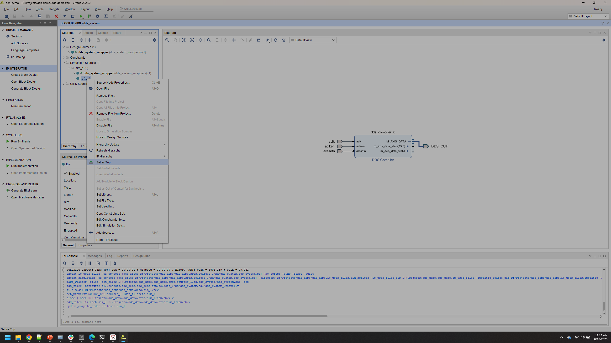
Right click the tb.v file in your Simulation Resources and select Set as Top. If your tb.v file is in Design Resources you probably didn’t specify the type of source you wanted to add correctly.
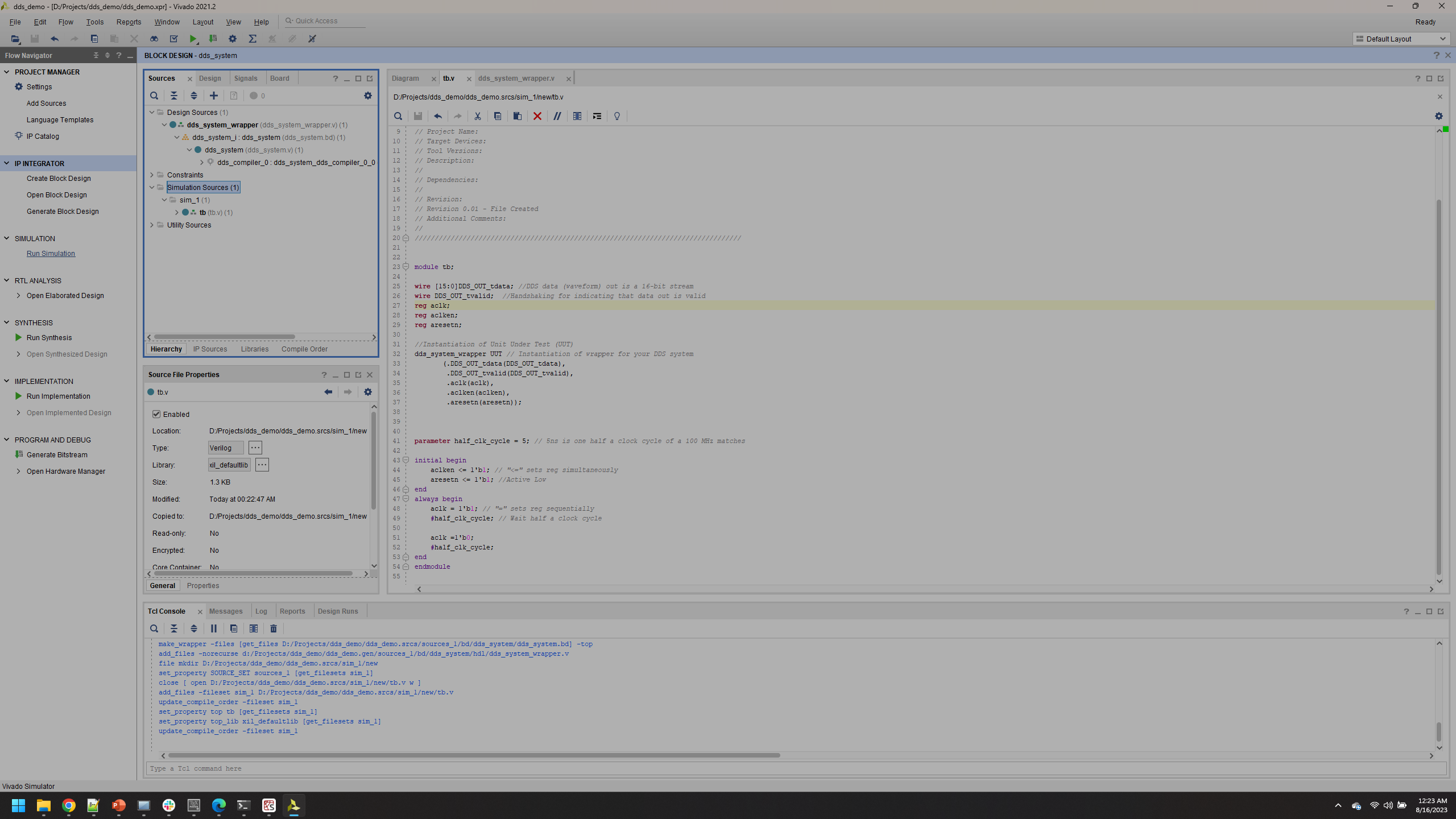
Double click tb.v to open it.
Update the tb.v file with the code below and save.
module tb;

wire [15:0]DDS_OUT_tdata; //DDS data (waveform) out is a 16-bit stream
wire DDS_OUT_tvalid;  //Handshaking for indicating that data out is valid
reg aclk;
reg aclken;
reg aresetn;

//Instantiation of Unit Under Test (UUT)
dds_system_wrapper UUT // Instantiation of wrapper for your DDS system
       (.DDS_OUT_tdata(DDS_OUT_tdata),
        .DDS_OUT_tvalid(DDS_OUT_tvalid),
        .aclk(aclk),
        .aclken(aclken),
        .aresetn(aresetn));

parameter half_clk_cycle = 5; // 5ns is one half a clock cycle of a 100 MHz matches

initial begin
    aclken <= 1'b1; // "<=" sets reg simultaneously
    aresetn <= 1'b1; //Active Low
end
always begin
    aclk = 1'b1; // "=" sets reg sequentially
    #half_clk_cycle; // Wait half a clock cycle

    aclk =1'b0;
    #half_clk_cycle;
end
endmodule
Click Run Simulation along the left side
Click Zoom Fit icon along the top tools.
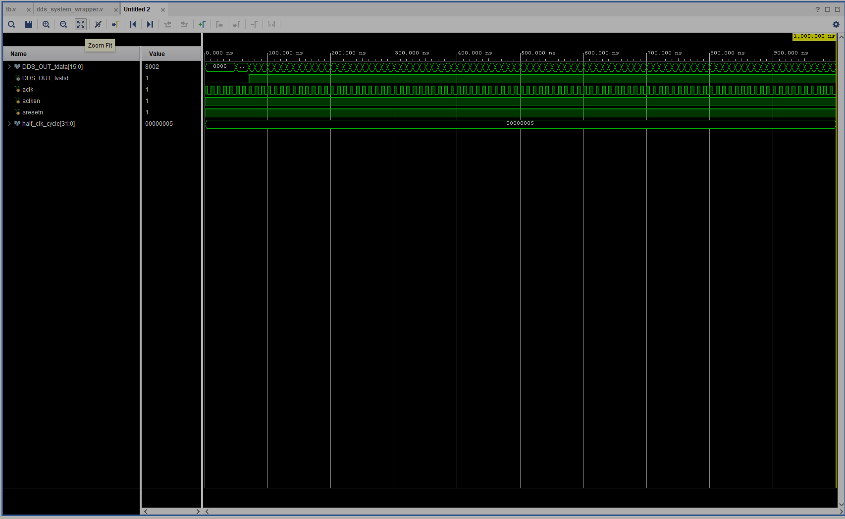
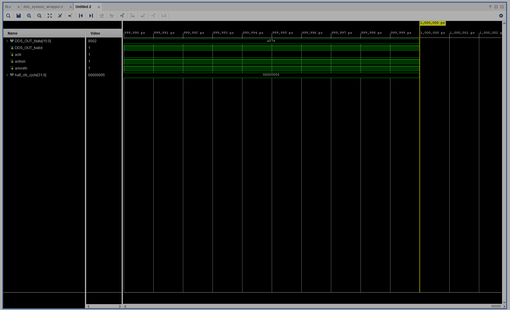
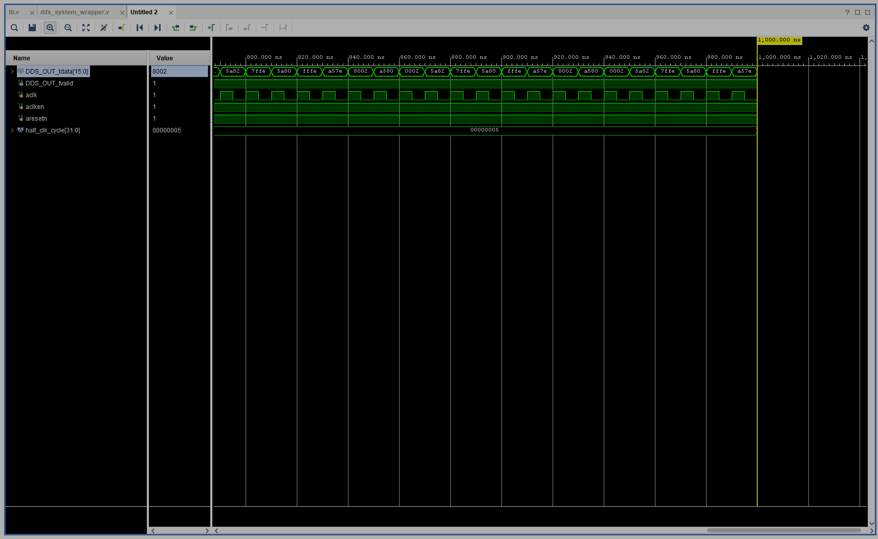
Click the Zoom In icon until you see the numbers pop up as below. Observe that every clock cycle (aclk if you followed the suggested naming convention), the DDS output changes value. However, this is not the ideal way to view a signal in the time domain.
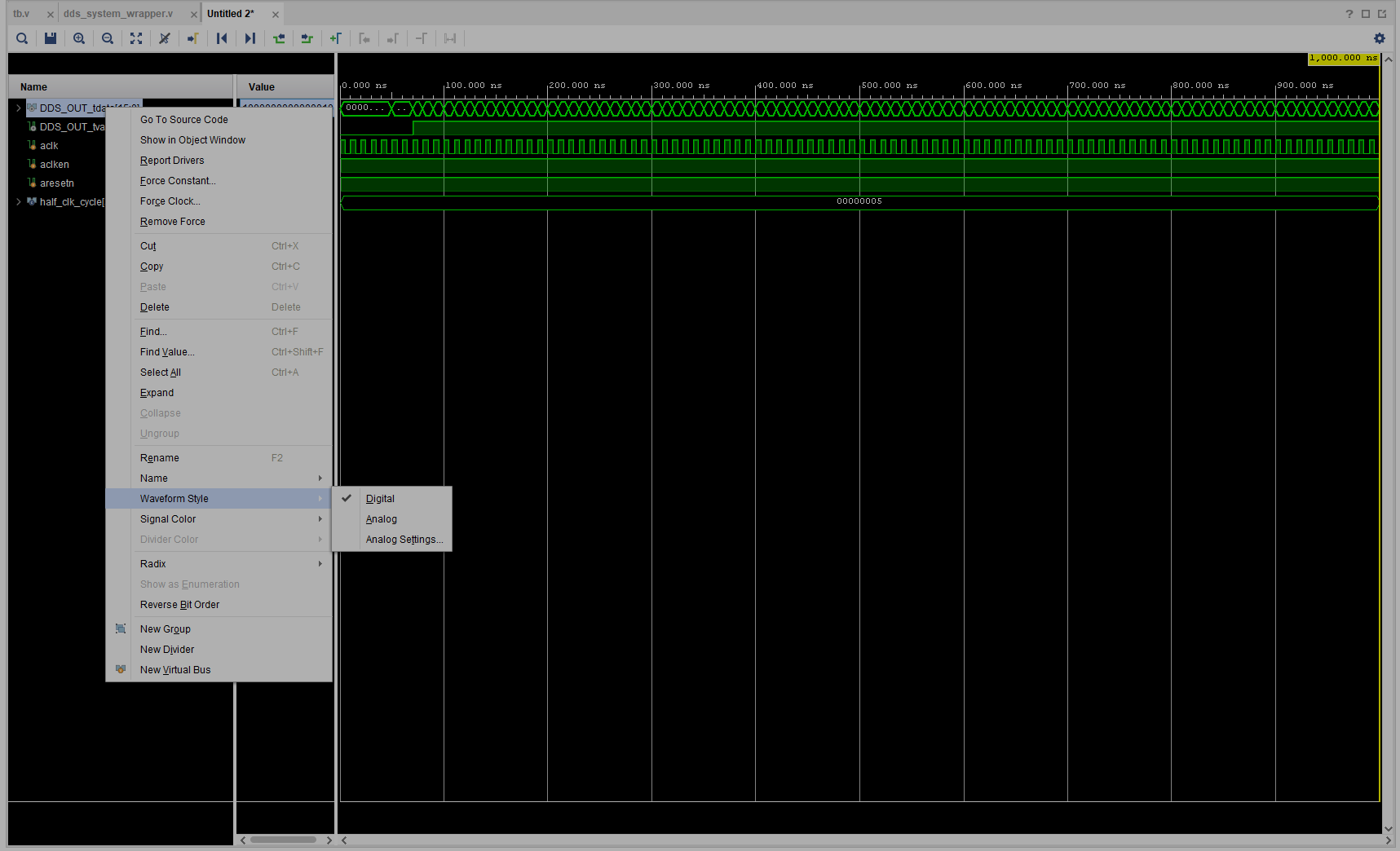
Right click the DDS out (DDS_OUT_tdata[15:0]), change Waveform Style from Digital to Analog.
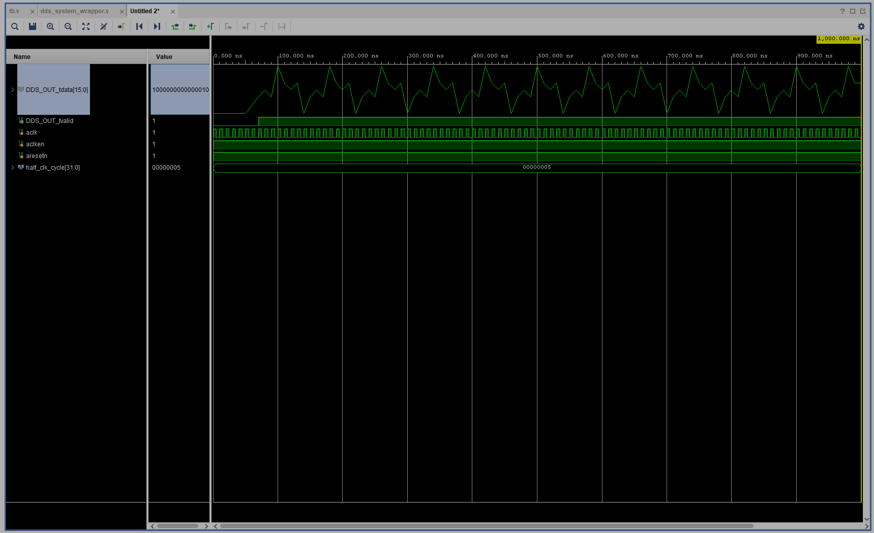
Ok what’s broken? Why is this not a clean sine wave? Actually, if you’re seeing what’s in the figure below, you just need to change your numerical representation. Remember the DDS generates values in twos-complement.
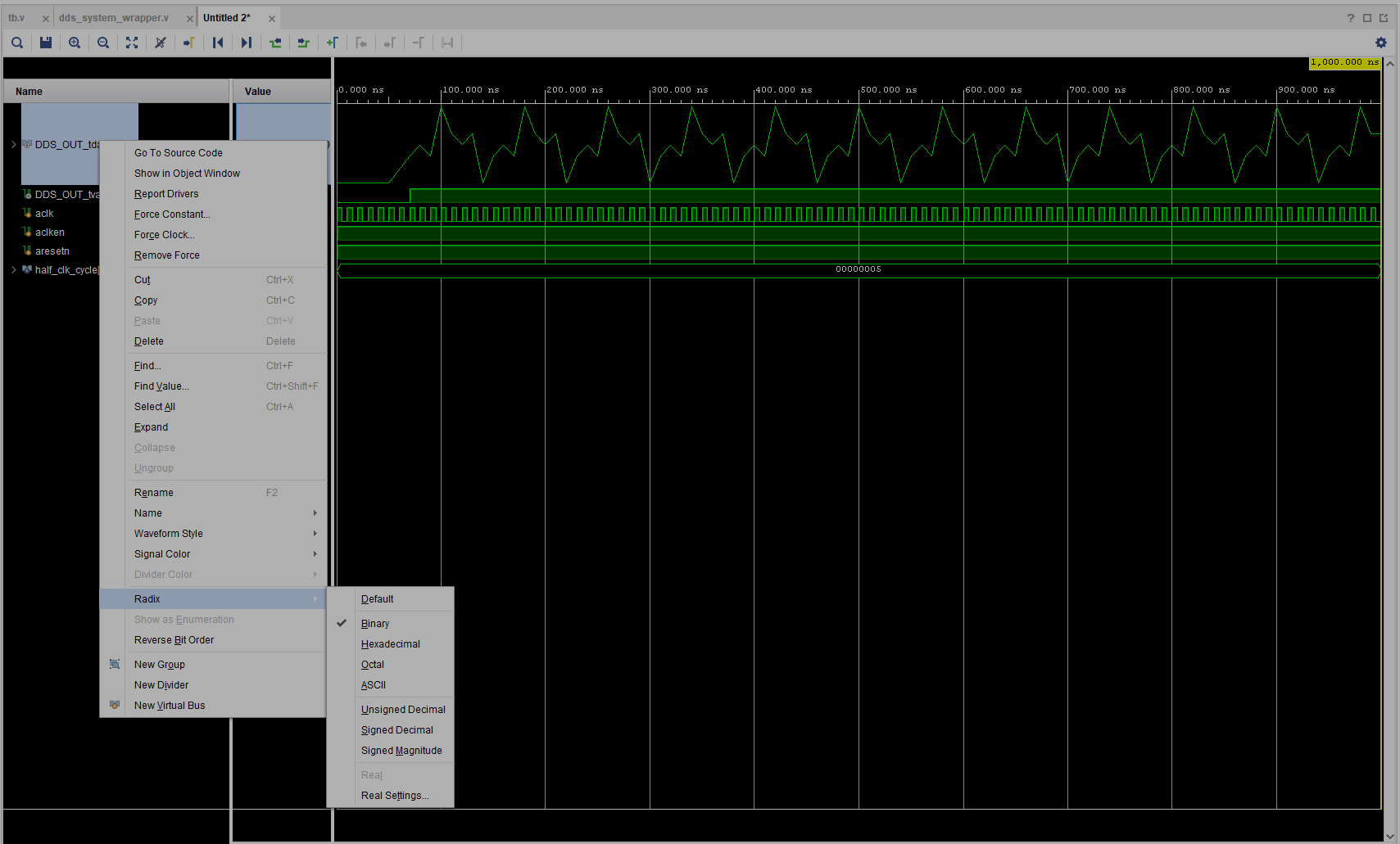
Right click the DDS out (DDS_OUT_tdata[15:0]), changing the Radix settings change the numbering scheme that appears in the individual cells each clock cycle. Change this to Signed Decimal
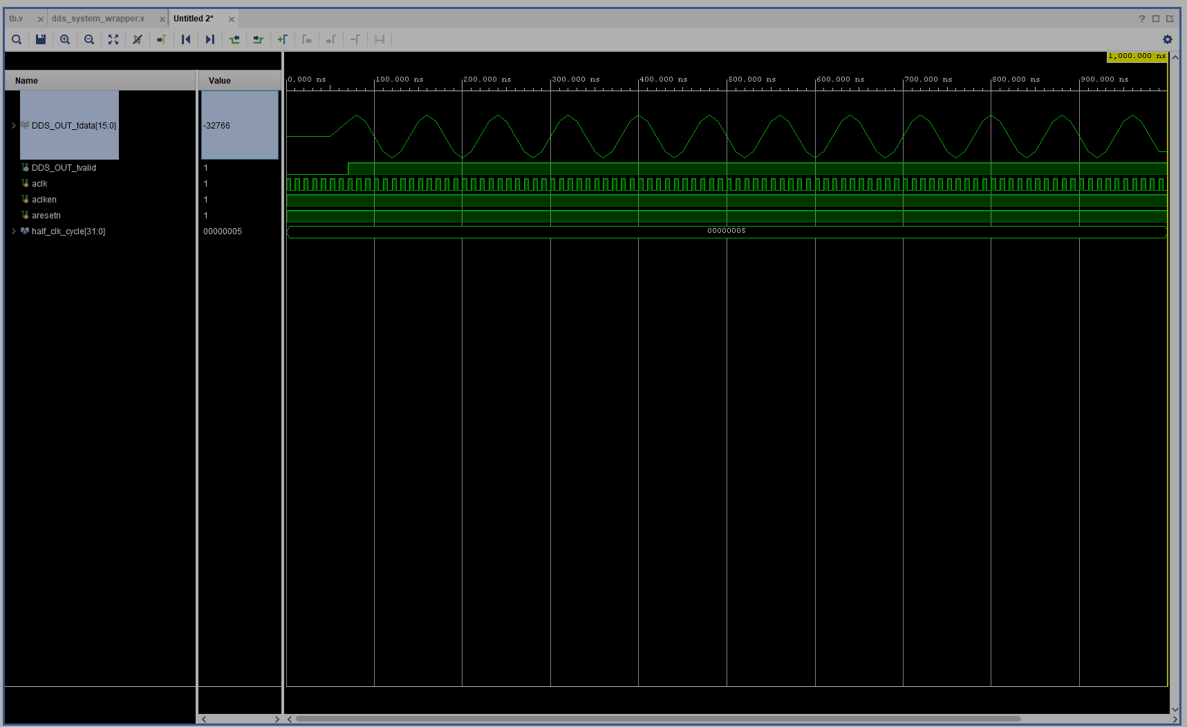
Voila.
Go ahead and close the simulation by clicking the X in the upper right on the blue banner (not for Vivado)
Click Open Block Design along the left side (or click the tab with your block design), and double click your DDS block.
Change the Phase Increment Value to the following (divide by 2).
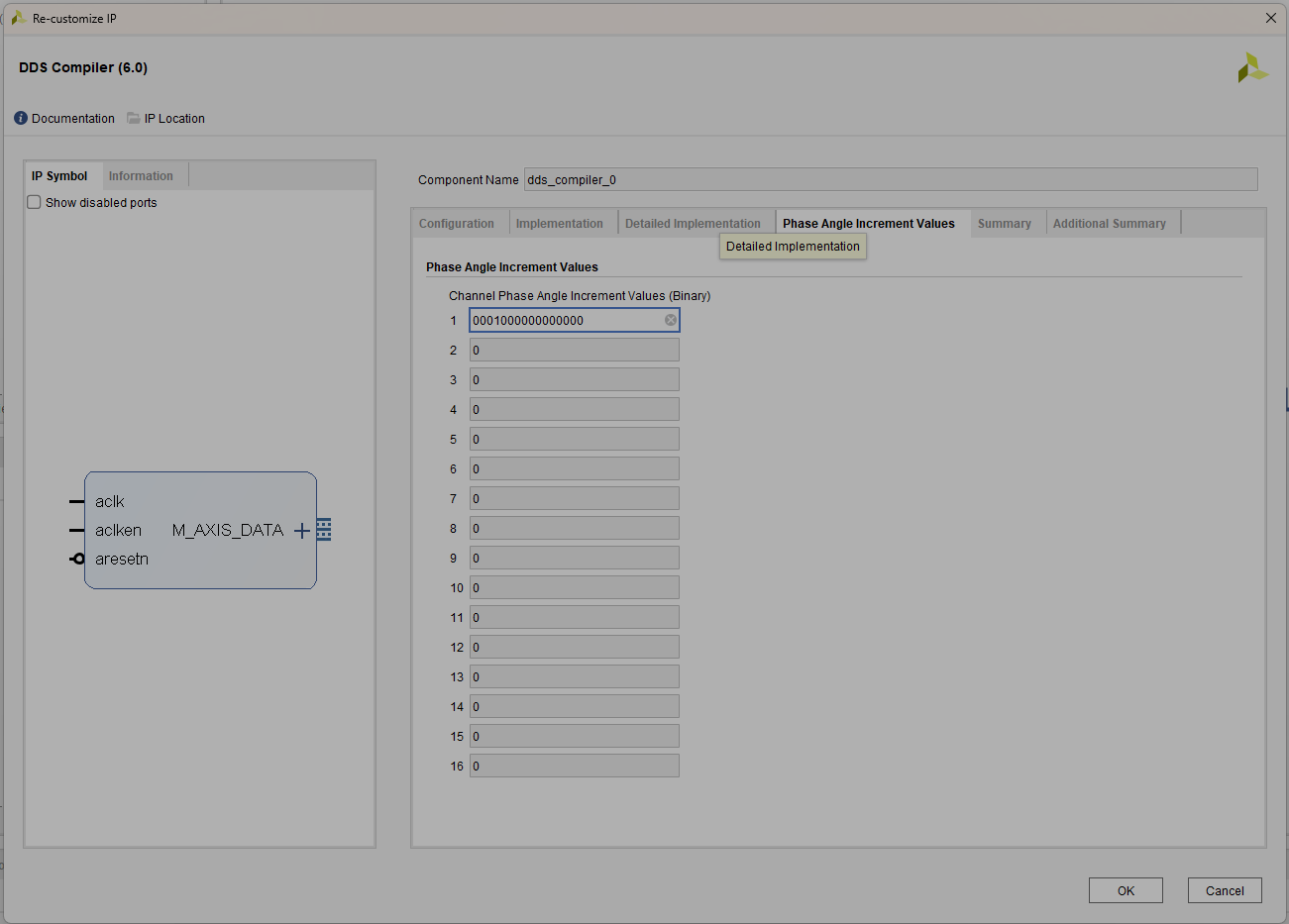
This should cut the previous frequency in half.
Click Ok and save.
Follow the previous steps to Run Simulation and visualize the waveform. Note the lower frequency sine wave.

Again, close the simulation by clicking the X in the upper right on the blue banner (not for Vivado)
Update HDL Wrapper
Click Open Block Design along the left side (or click the tab with your block design), and double click your DDS block.
Up to this point you have designed waveform generators with fixed frequencies, but in reality, signals are dynamic in phase, frequency, and amplitude. This last section details how to add an interface port to your DDS block such that you may stream frequency values over time. This enables generation of waveforms that possess linear frequency modulation (LFM), for example.
In the Implemention tab, change the Phase Increment Programmability to Streaming, this will add a port.
Click OK
Right click the text for the new port and click Make External, change the name as shown below.
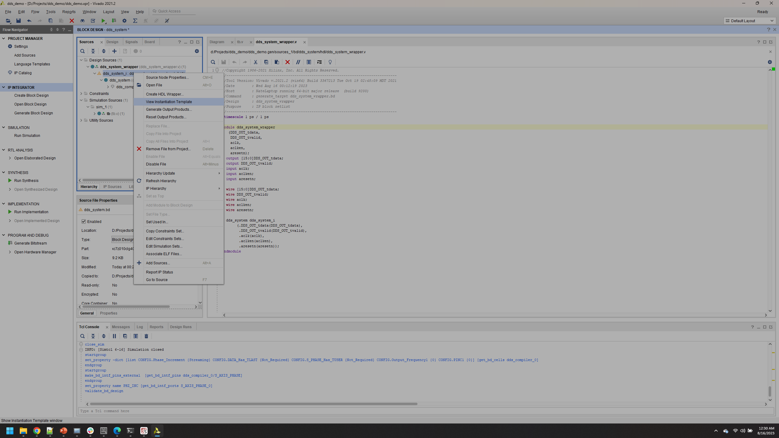
Double click the HDL wrapper created previously, note that the new port is likely not added. This an ongoing issue with Vivado…
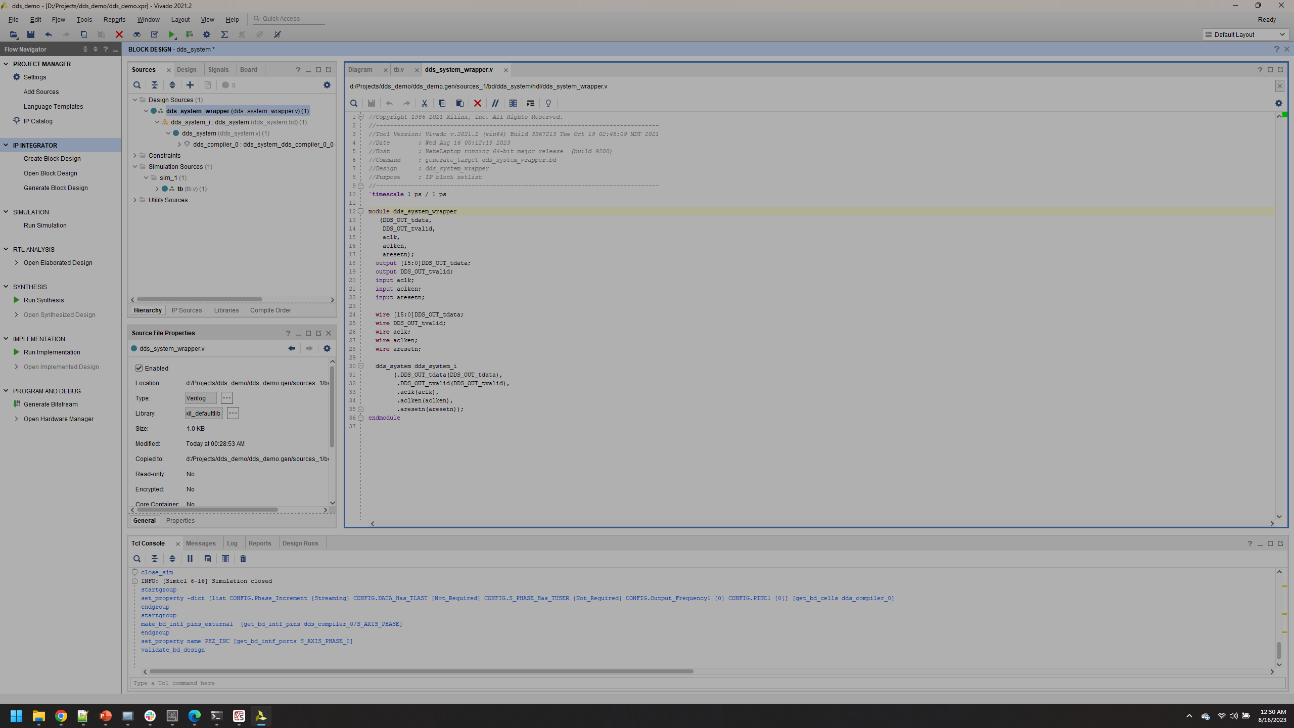
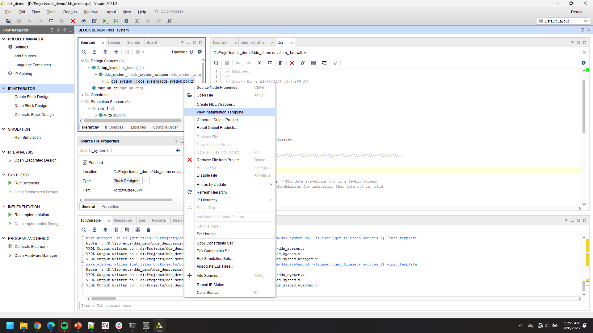
A workaround our team uses is to expand the drop down under the HDL wrapper file and right click the block diagram design within. In the pop-up menue, click View Instantiation Template, which forces an update.
When the banner displaying This file has been changed. Reload appears, click Reload.
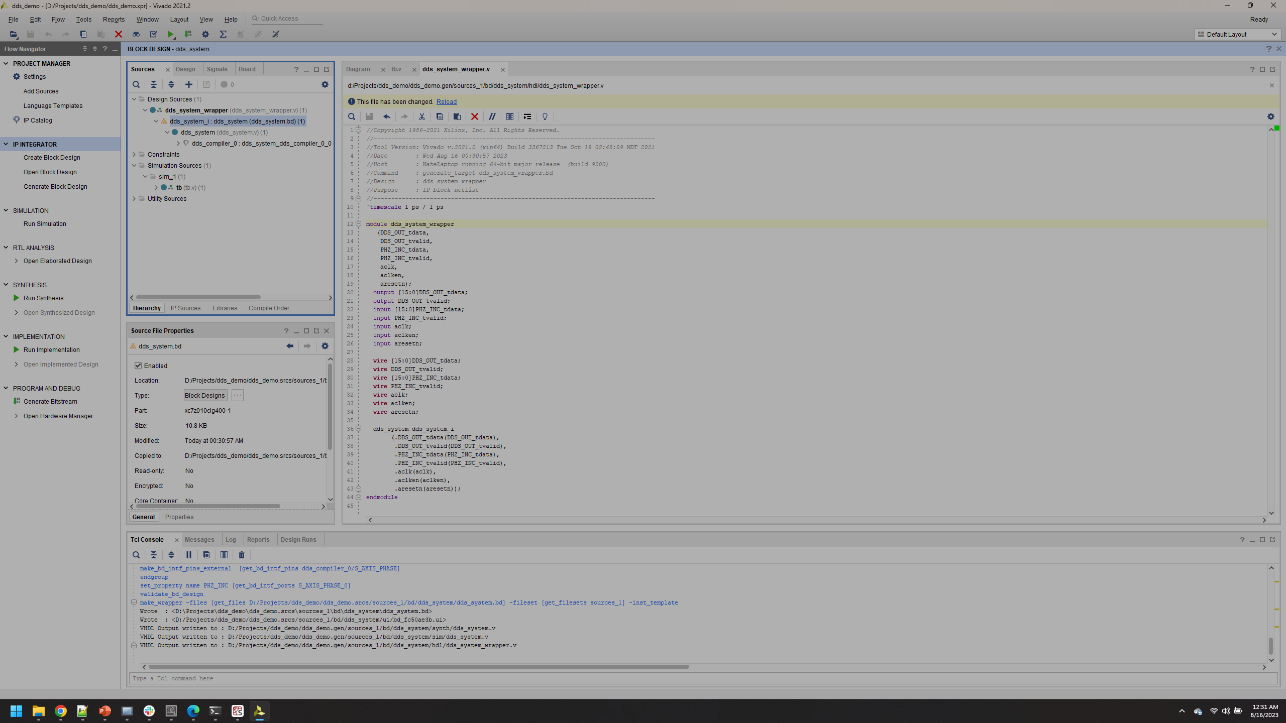
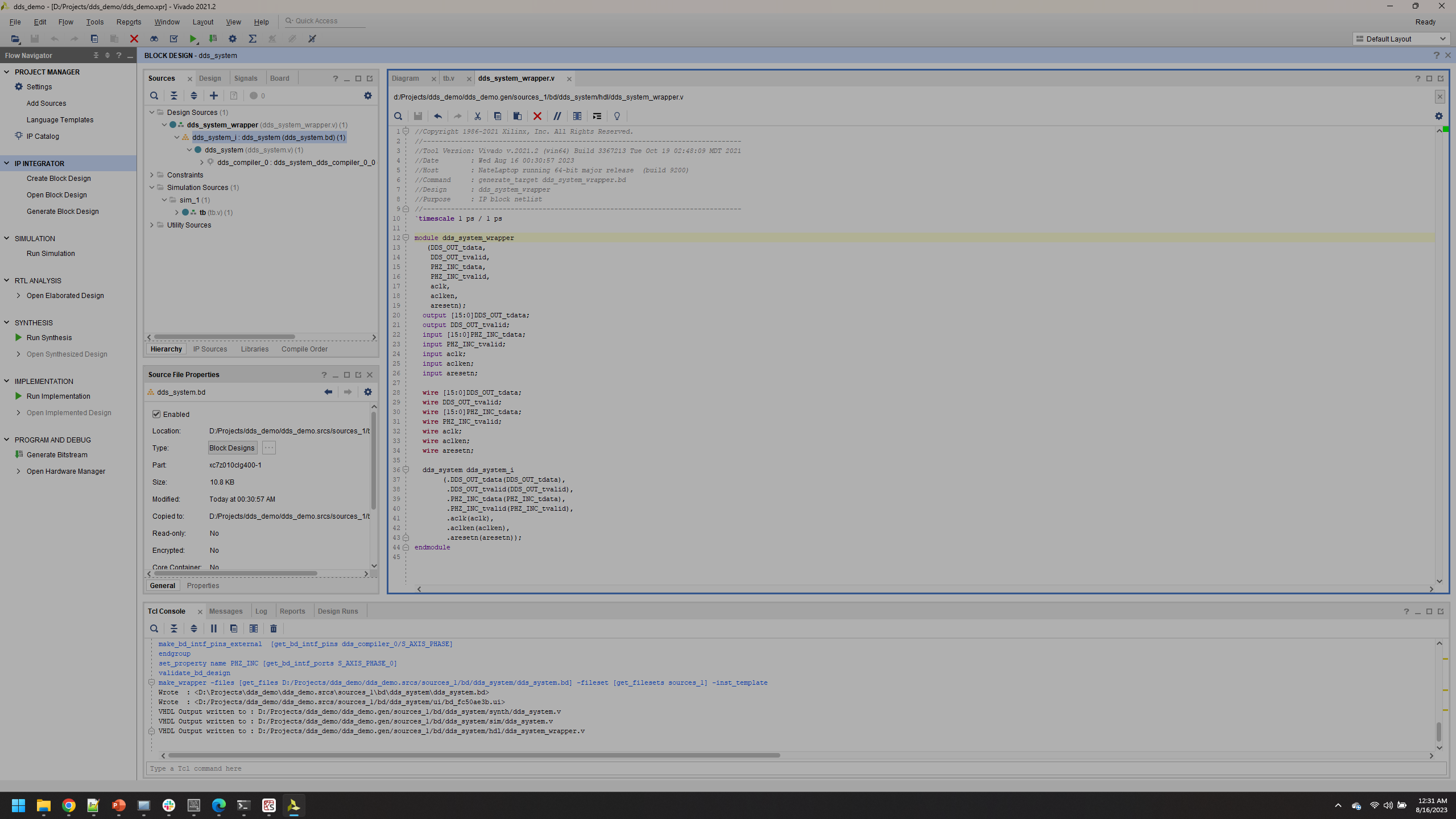
Now that that is dealt with, the new port should appear for lines 15-16. Note that two ports are required for the AXI interface (more detail in another tutorial).
Changing the Frequency
Update the tb.v under your Simulation Resources with the following code:
module tb;

wire [15:0]DDS_OUT_tdata; //DDS data (waveform) out is a 16-bit stream
wire DDS_OUT_tvalid;  //Handshaking for indicating that data out is valid
reg aclk;
reg aclken;
reg aresetn;

//***************************************************UPDATE************
reg [15:0]PHZ_INC_tdata;
reg PHZ_INC_tvalid;
//*********************************************************************


//Instantiation of Unit Under Test (UUT)
dds_system_wrapper UUT
       (.DDS_OUT_tdata(DDS_OUT_tdata),
        .DDS_OUT_tvalid(DDS_OUT_tvalid),

        //***************************************************UPDATE************
        .PHZ_INC_tdata(PHZ_INC_tdata),
        .PHZ_INC_tvalid(PHZ_INC_tvalid),
        //*********************************************************************

        .aclk(aclk),
        .aclken(aclken),
        .aresetn(aresetn));


parameter half_clk_cycle = 5; // 5ns is one half a clock cycle of a 100 MHz matches

initial begin
    aclken <= 1'b1; // "<=" sets reg simultaneously
    aresetn <= 1'b1; //Active Low

    //***************************************************UPDATE************
    PHZ_INC_tdata <= 16'b0001_0000_0000_0000;
    PHZ_INC_tvalid <= 1'b1;
    //*********************************************************************

end
always begin
    aclk = 1'b1; // "=" sets reg sequentially
    #half_clk_cycle; // Wait half a clock cycle

    aclk =1'b0;
    #half_clk_cycle;
end
endmodule
Click Run Simulation and observe that you get 6.25 MHz sine wave. Adjust zoom and settings as usual to visualize the waveform.
Ok, so what? Well now you have a block in which you can interface and change the frequency at any required clock cycle periodically at each clock cycle.
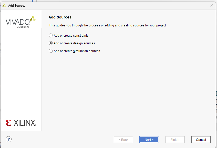
It’s generally good practice to work from a “Top Level” HDL file to manage your project. Right click Design Sources and click Add Sources.
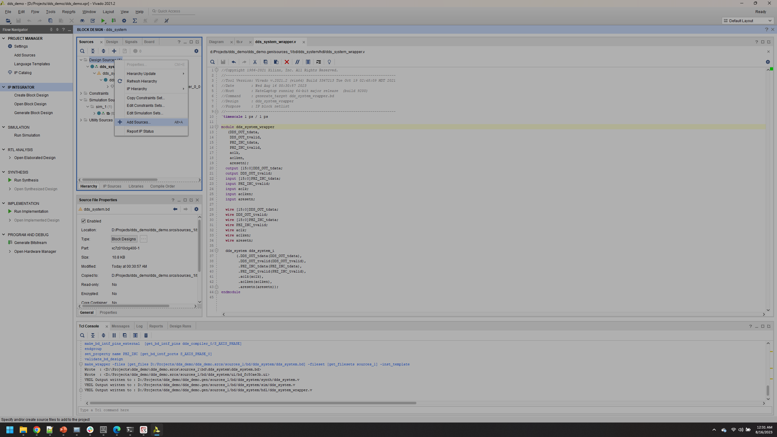
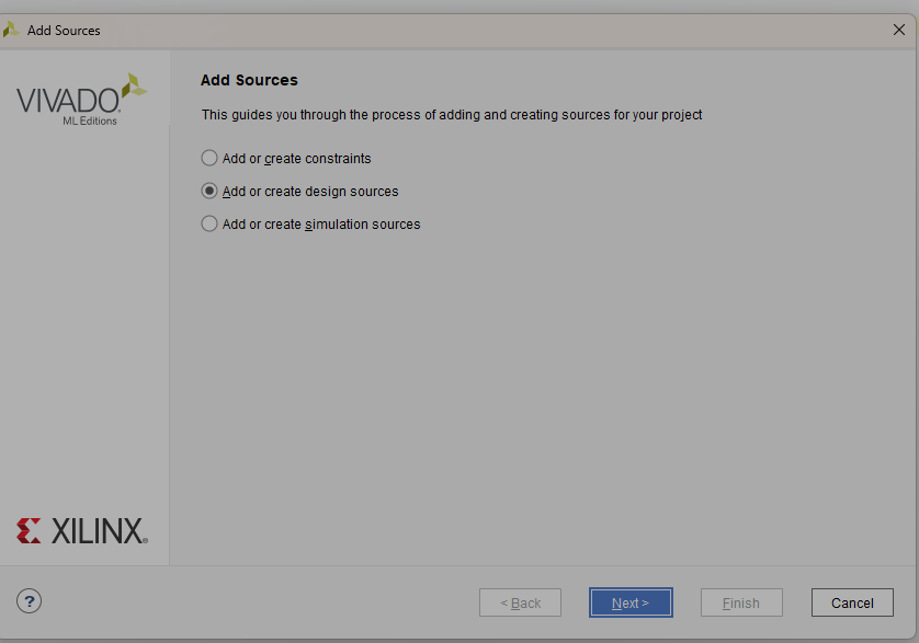
Click Next.
Click Create File, name it `top_level`.
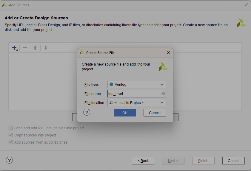
Click OK
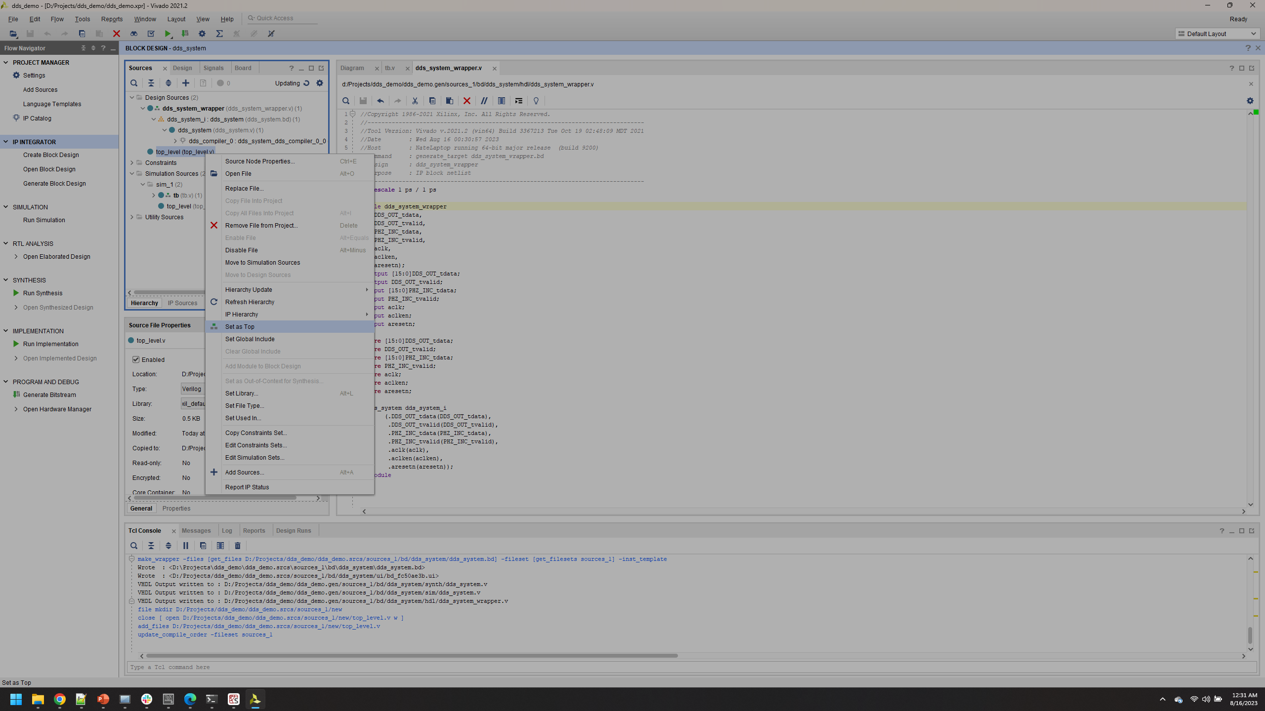
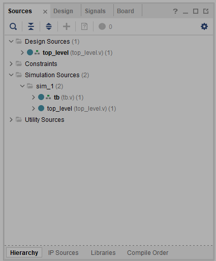
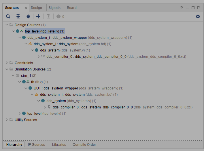
Right click your `top_level.v` module and select Set as Top.
Copy paste from `dds_system_wrapper.v` and paste it into `top_level.v`. The code is included after the figures to avoid issues.
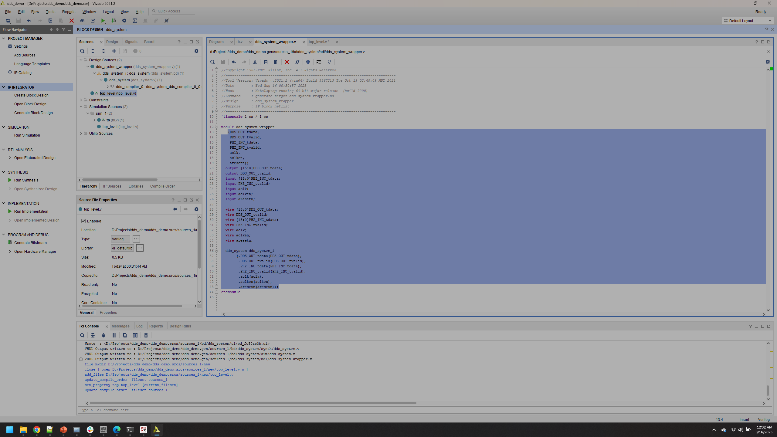
Click Save, observe that `top_level.v` is now encompassing of all project elements in the hierarchy.
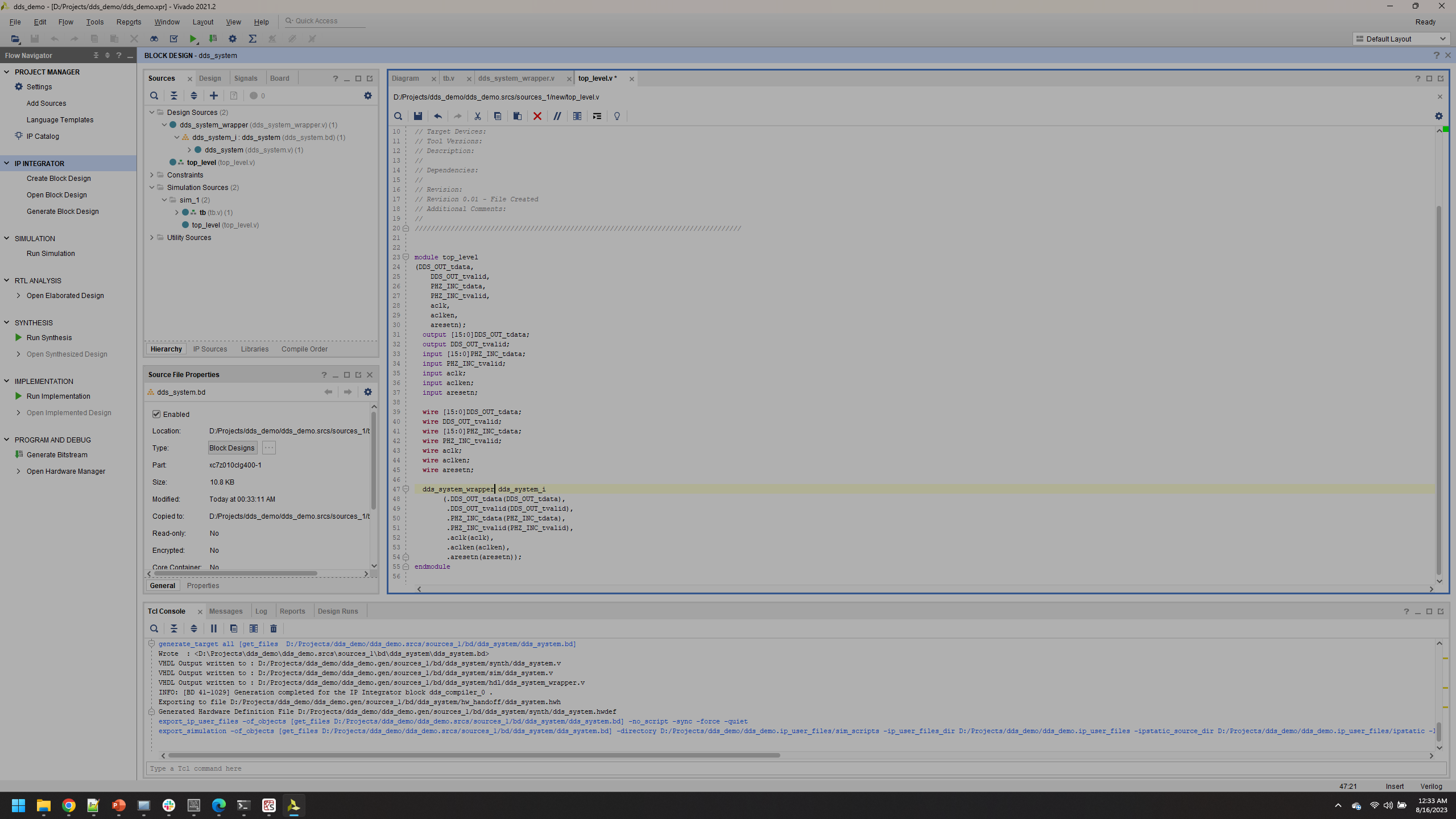
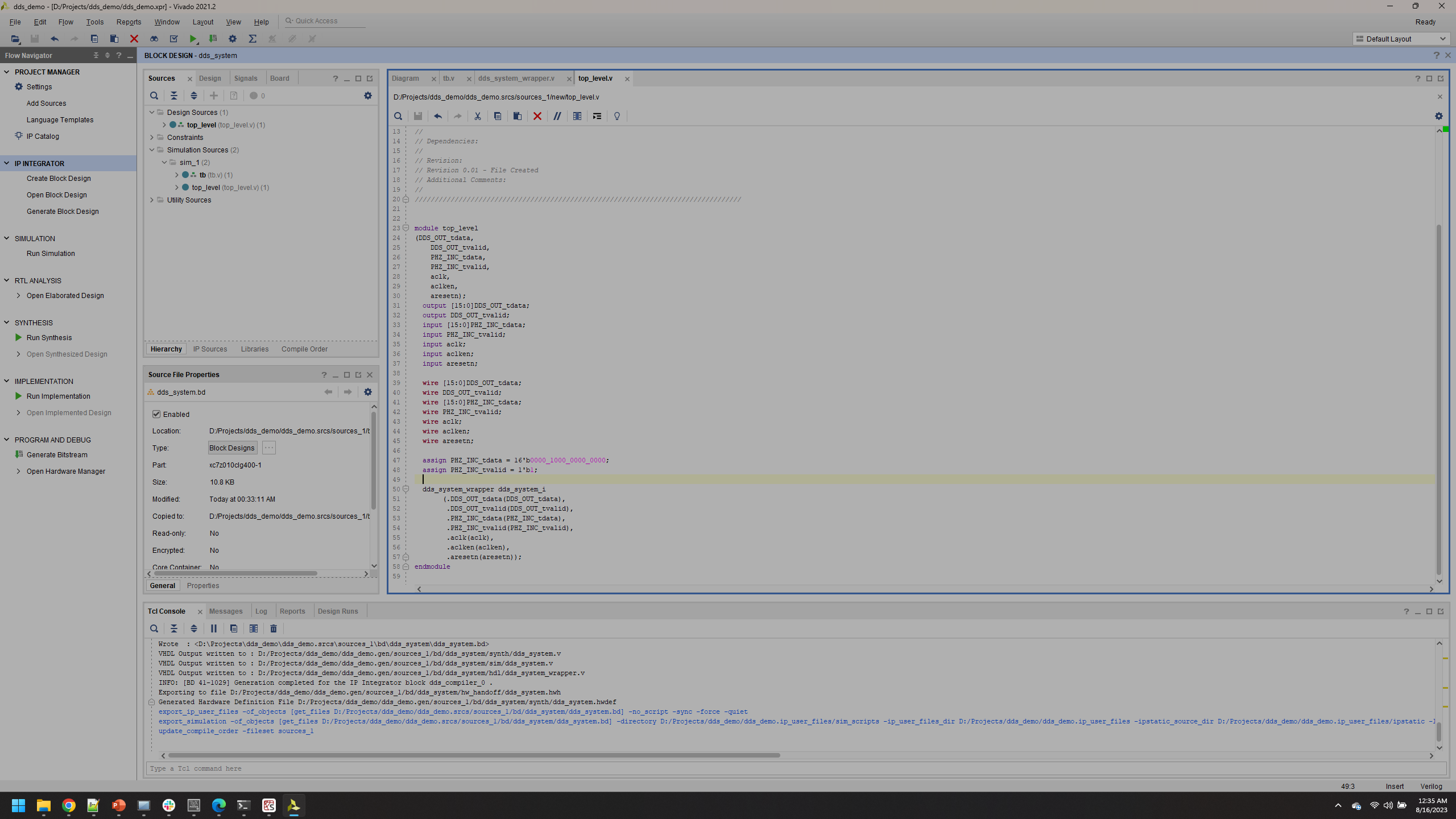
Update top_level.v with the following lines in 47-48 as shown below
module top_level
(DDS_OUT_tdata,
    DDS_OUT_tvalid,
    PHZ_INC_tdata,
    PHZ_INC_tvalid,
    aclk,
    aclken,
    aresetn);
  output [15:0]DDS_OUT_tdata;
  output DDS_OUT_tvalid;
  input [15:0]PHZ_INC_tdata;
  input PHZ_INC_tvalid;
  input aclk;
  input aclken;
  input aresetn;

  wire [15:0]DDS_OUT_tdata;
  wire DDS_OUT_tvalid;
  wire [15:0]PHZ_INC_tdata;
  wire PHZ_INC_tvalid;
  wire aclk;
  wire aclken;
  wire aresetn;

  assign PHZ_INC_tdata = 16'b0000_1000_0000_0000;
  assign PHZ_INC_tvalid = 1'b1;

  dds_system_wrapper dds_system_i
       (.DDS_OUT_tdata(DDS_OUT_tdata),
        .DDS_OUT_tvalid(DDS_OUT_tvalid),
        .PHZ_INC_tdata(PHZ_INC_tdata),
        .PHZ_INC_tvalid(PHZ_INC_tvalid),
        .aclk(aclk),
        .aclken(aclken),
        .aresetn(aresetn));
endmodule
Pulse Control
Create a new design resource, right click Design Resources and from the drop down click Add Source, make sure in the menu that follows you specify Design Source
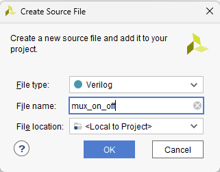
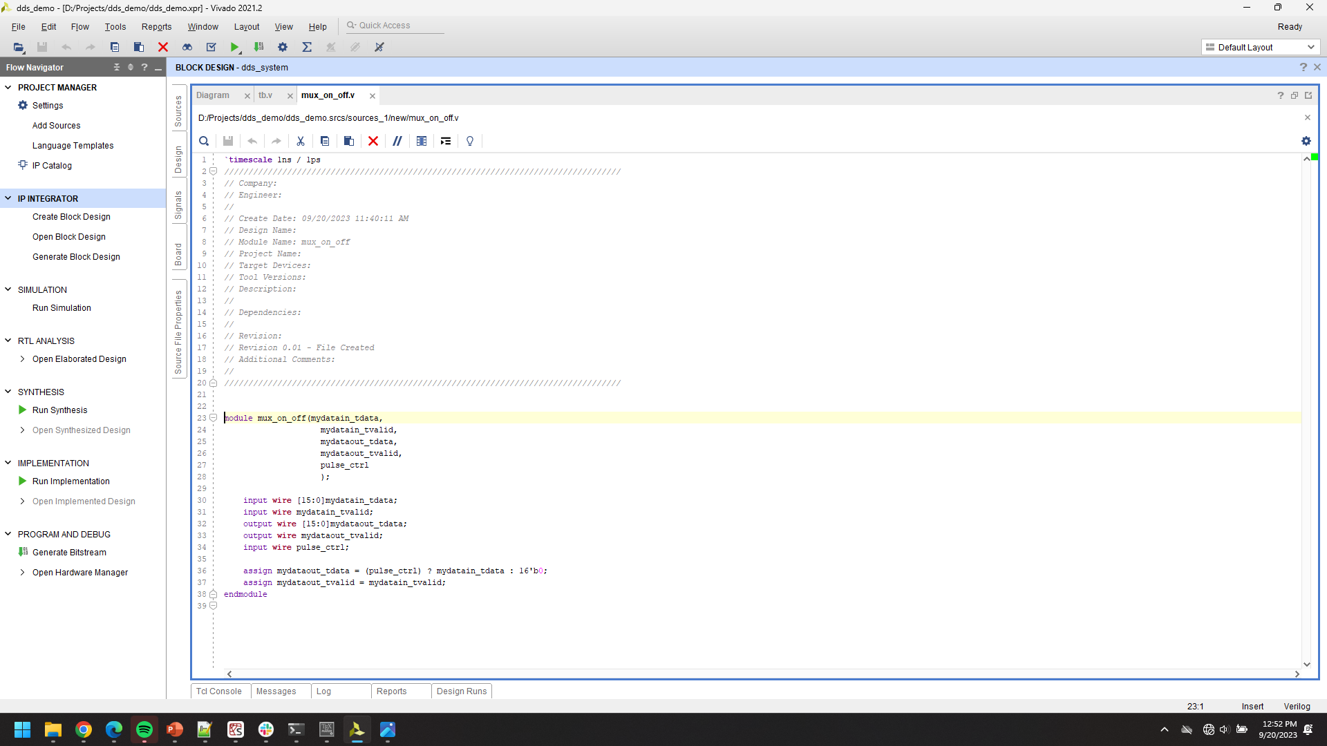
Copy paste the following code into the mux_on_off.v file
module mux_on_off(mydatain_tdata,
                    mydatain_tvalid,
                    mydataout_tdata,
                    mydataout_tvalid,
                    pulse_ctrl
                    );

    input wire [15:0]mydatain_tdata;
    input wire mydatain_tvalid;
    output wire [15:0]mydataout_tdata;
    output wire mydataout_tvalid;
    input wire pulse_ctrl;

    assign mydataout_tdata = (pulse_ctrl) ? mydatain_tdata : 16'b0;
    assign mydataout_tvalid = mydatain_tvalid;
endmodule
Click and Drag the new source mux_on_off.v in to the block diagram
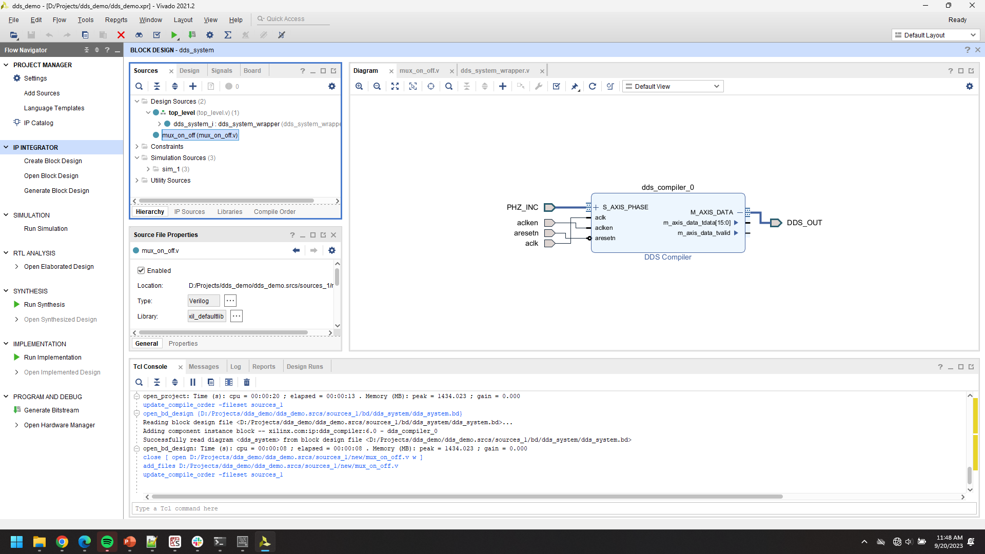
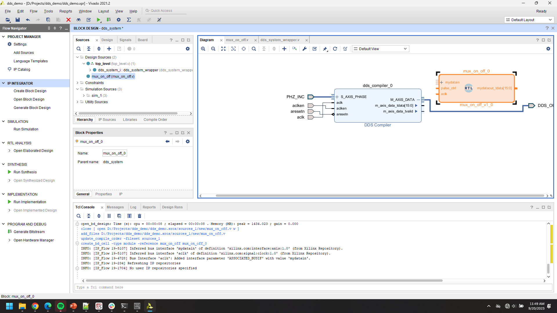
Click the wire conneciting the DDS module to the output port DDS_OUT, press DELETE.
Note that you will not have an aclk input for your version.
Reconnect the block diagram as shown below, ignore the aclk port portions.
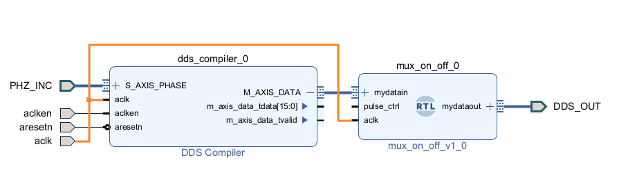
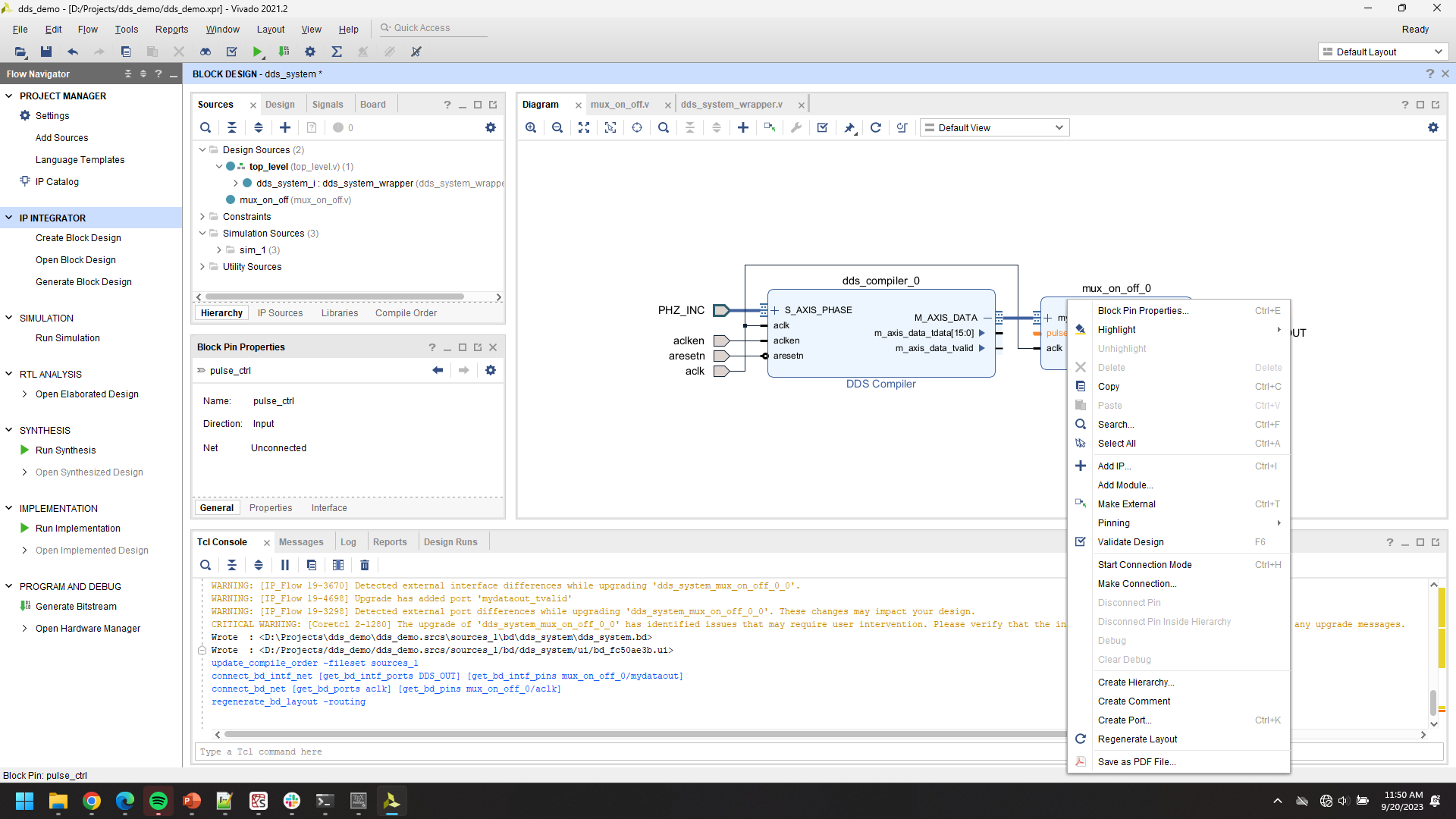
Right click the text on your mux block and click Make External
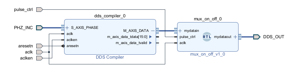
You will need to update the HDL wrapper as you did before.
Update your tb.v in your simulation sources with the code below and save.
module tb;

wire [15:0]DDS_OUT_tdata; //DDS data (waveform) out is a 16-bit stream
wire DDS_OUT_tvalid;  //Handshaking for indicating that data out is valid
reg aclk;
reg aclken;
reg aresetn;

reg [15:0]PHZ_INC_tdata;
reg PHZ_INC_tvalid;
reg pulse_ctrl;
reg [8:0]counter = 9'b0;
reg [1:0] state, next_state;

//State machine parameters governing pulse on/off
parameter num_clock_cycles_on = 100;
parameter num_clock_cycles_off = 400;
parameter PULSE_HIGH = 1'b1, PULSE_LOW = 1'b0;

//Instantiation of Unit Under Test (UUT)
dds_system_wrapper UUT
       (.DDS_OUT_tdata(DDS_OUT_tdata),
        .DDS_OUT_tvalid(DDS_OUT_tvalid),
        .PHZ_INC_tdata(PHZ_INC_tdata),
        .PHZ_INC_tvalid(PHZ_INC_tvalid),
        .aclk(aclk),
        .aclken(aclken),
        .aresetn(aresetn),
        .pulse_ctrl(pulse_ctrl));


parameter half_clk_cycle = 5; // 5ns is one half a clock cycle of a 100 MHz matches

initial begin
    aclken <= 1'b1; // "<=" sets reg simultaneously
    aresetn <= 1'b1; //Active Low
    PHZ_INC_tdata <= 16'b0000_1000_0000_0000;
    PHZ_INC_tvalid <= 1'b1;
    pulse_ctrl <= 1'b1;
    next_state <= PULSE_HIGH;
end
always @(posedge aclk) begin
    state = next_state;
    case (state)
        PULSE_HIGH: begin
            if (counter < num_clock_cycles_on) begin
                counter <= counter + 1'b1;
            end else begin
                counter = 9'b0;
                next_state = PULSE_LOW;
                pulse_ctrl = 1'b0;
            end
        end
        PULSE_LOW: begin
            if (counter < num_clock_cycles_off) begin
                counter <= counter + 1'b1;
            end else begin
                counter = 9'b0;
                next_state = PULSE_HIGH;
                pulse_ctrl = 1'b1;
            end
        end
    endcase
end
always begin
    aclk = 1'b1; // "=" sets reg sequentially
    #half_clk_cycle; // Wait half a clock cycle

    aclk =1'b0;
    #half_clk_cycle;
end
endmodule
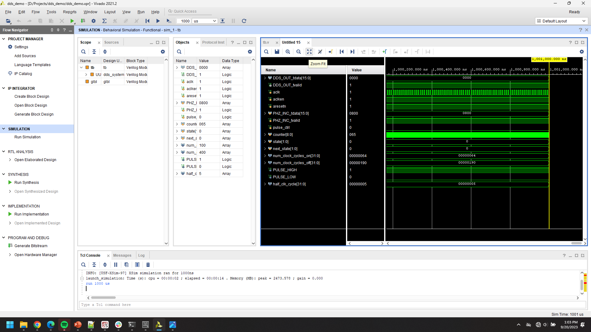
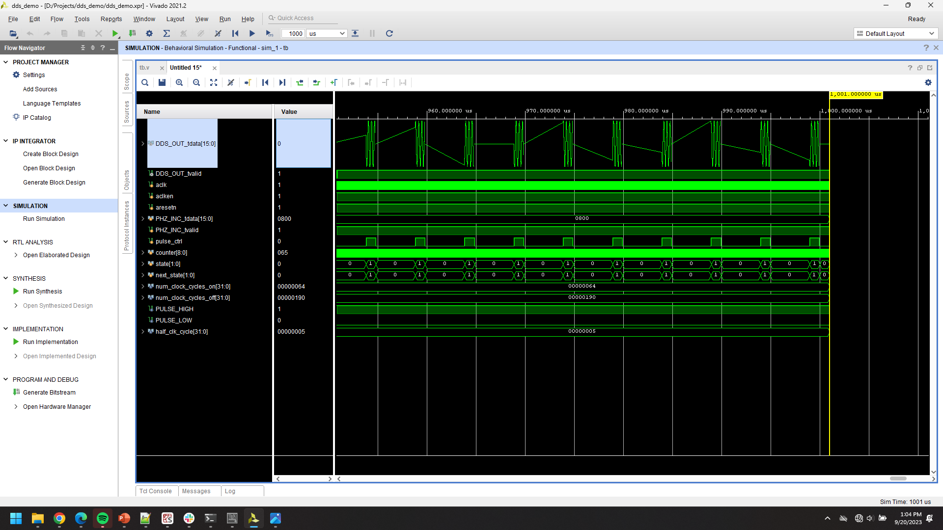
Save and Run Simulation
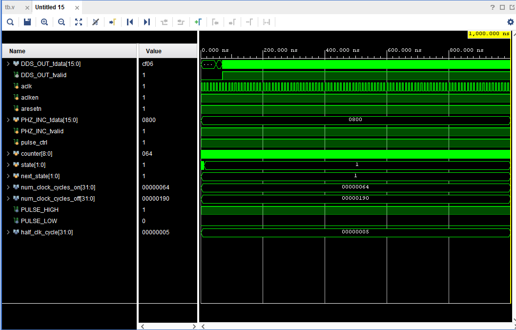
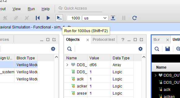
Use the simulation settings toolbar to change the run time to 1000 us. Press to run.
Adjust the zoom and timing window settings as you’ve done previously, as well as the signal display (analog vs digital, signed decimal, etc.).